ISFH SolarTeC
Industrial processing tools
Contact
Dr. Thorsten Dullweber
Head of PV department for Infrastructure
Tel.: +49(0)5151-999 642
E-Mail: dullweber@isfh.de

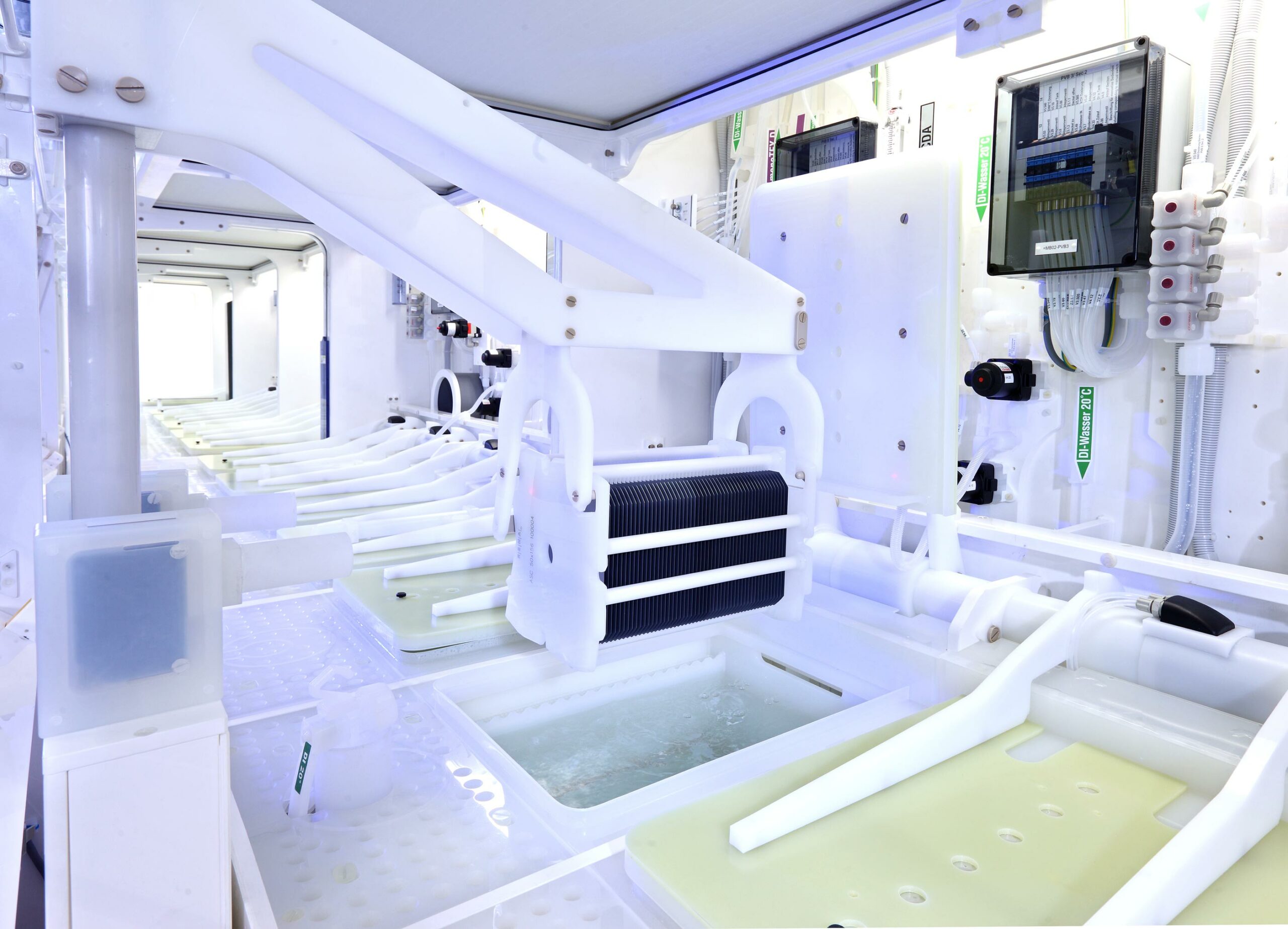
Tool for wet chemical processing (RENA Batchlab)

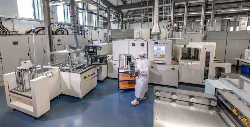
Screen printing island for fully automated screen printing on silicon solar cells.

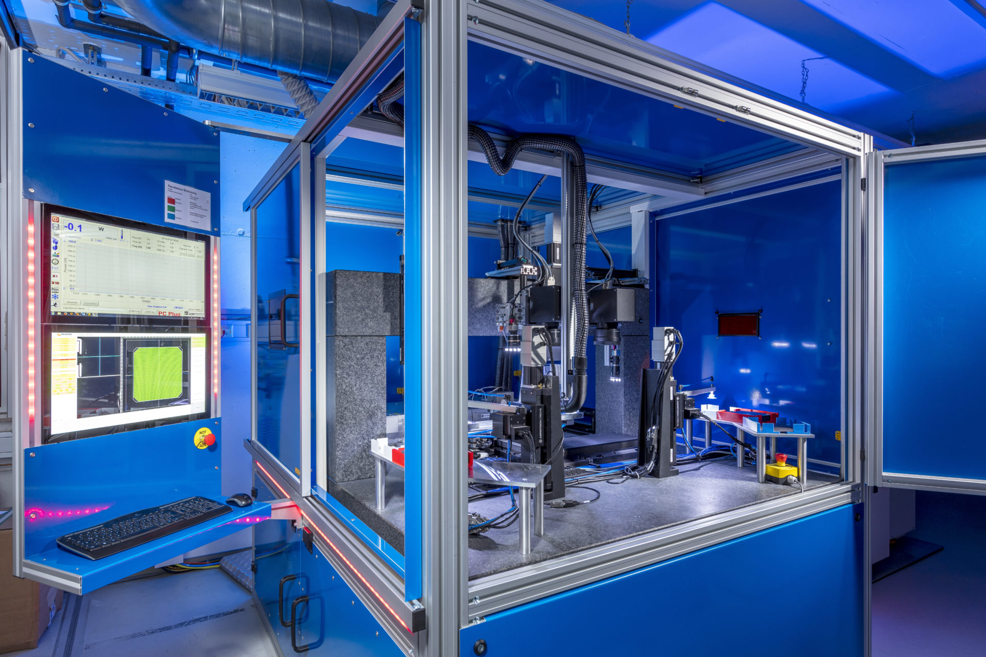
Laser tool with picosecond pulse length
In the ISFH SolarTeC, we process large-area solar cells in a near-production environment on industry-relevant equipment. The heart of this infrastructure is the 800 m² technology centre, which houses tools for wet chemistry, diffusion, oxidation, PECVD, ALD, screen-printing metallization and module production. The technology centre is supplemented by further laboratories for laser processes and industrial LPCVD processing tools.
At ISFH we pursue an industry-oriented approach of developing new technologies ideally as drop-in or add-on for today’s industrial mainstream. Current examples are passivating “poly-Si-on-oxide” (POLO) contacts and tandem cell concepts. This is achieved through close cooperation between all groups in the photovoltaics department.
A particular strength of ISFH’s SolarTeC is its flexibility. We have many years of experience in comparing our partners’ processes and systems using cross-processing with our reference processes and equipment in the SolarTeC. This offers our partners the opportunity to evaluate specific materials and individual process steps or to develop alternative cell and module concepts together with us.
Tool list
- Batch tool for wet chemical cleaning, Si etching, and alkaline texturing (RENA)
- Inline tool for single side polishing and etching (RENA)
- Quartz tube furnace for thermal oxidation as well as POCL3– and BBr3-diffusion (Tempress)
- LPCVD-furnace for deposition of a-Si (Centrotherm)
- Direct PECVD for SiNx deposition (Roth&Rau)
- Industrial PECVD tool for SiNx, AlOx and poly-Si deposition (Centrotherm)
- Ultra-fast ALD tool (SolayTec)
- Laser laboratory with five laser material processing systems, e.g. for ablation of dielectric layers or laser doping (InnoLas, Coherent, IPG, EdgeWave, Trumpf)
- Industrial screen printers and firing furnaces for the solar cell metallization (DEK, ASYS, centrotherm)
- Integrated inline high-rate evaporation and sputtering system (Applied Materials)
- MultiWire-Foilator and Assembling for interconnection of busbarless cells (Meyer Burger)
- Vacuum laminator (Meier)
Examples of successful technology development on large-area solar cells at SolarTeC
- POLO BJ solar cells with LPCVD poly-Si with 24.2% efficiency (2023)
- POLO IBC solar cell with local PECVD SiON/n-a-Si deposition through shadow mask with 23.8% efficiency (2023)
- Bifacial PERC+ solar cells with aluminium finger grid on the back and efficiencies of up to 23.2% (2022)
- Double-side contacted, screen-printed solar cells with POLO contacts for both polarities and current efficiencies of up to 22.3% (in cooperation with Centrotherm, Leibniz Universität Hannover and Meyer Burger)
- Partial processing of a Si-bottom cell of a Si/III-V multijunction device with an efficiency of 35.4% (2017, interfacial oxide growth and POLO junction formation in the SolarTeC, subsequent cutting of the 156mm × 156mm Cz-Si wafer)
- Bifacial minimodule made of PERC+ solar cells and SmartWire technology with a module efficiency of 19.8% and a rear side efficiency of 16.4% (2016)
- PV module with 120 PERC half cells and 5 busbars with 20.2% efficiency (2015)
- Ion-implanted, screen-printed n-PERT solar cells with >99% bifacility and efficiencies up to 21.8% (2015, in cooperation with Leibniz Universität Hannover)
- Ion-implanted IBC (Interdigitated Back Contact) solar cells with efficiencies of up to 22.1% (2013, in cooperation with Bosch SE)
Examples of individual processes
Wet-chemical processes
- Etch-back of saw damage or highly doped surfaces
- Alkaline texture
- PSG/BSG etch
- RCA cleaning
- HF/HCl cleaning
- Chemical polishing
- Edge isolation
- One-sided etching of SiOx
Deposition
- PECVD-SiN, AlOx, poly-Si
- LPCVD of a-Si
- Plasma and Spatial ALD AlOx
- TCO
Laser processing
- Ablation of dielectric layers
- Laser doping to form the selective emitter or front surface field
- Melting of metallic or metal-containing layers for electrical (LFC) and/or mechanical (AMELI) contacting
- Cutting, drilling and marking of silicon, glass and metallic foils
High-temperature processes
- Phosphorus diffusion (POCl3)
- Boron diffusion (BBr3)
- Oxidation (wet and dry)
- Annealing process after ion implantation
- Formation of POLO contacts
Metallization
- Screen printing (single, dual, triple print)
