Laser
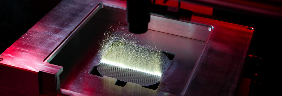
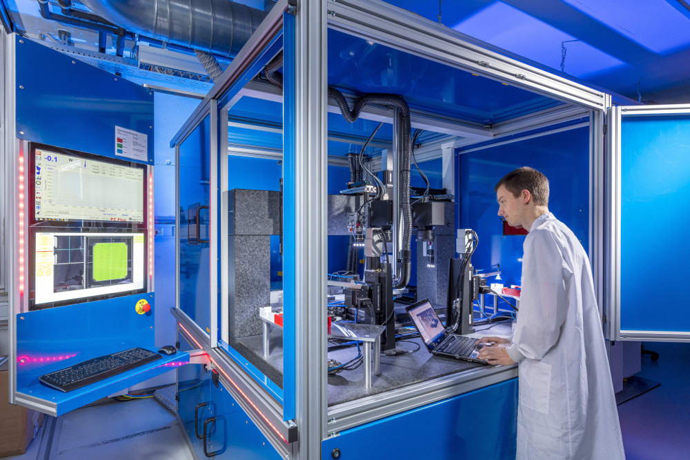
At ISFH we have five different laser systems for material processing that operate in a spectral range from IR to VIS to UV. The pulse length ranges from 1 us to below 10 ps.
All tools are capable of handling substrates with an edge length of up to 156 mm and have camera systems for positioning and aligning.
Typical applications include
- Ablation of dielectric layers for formation of contacts (laser contact opening, LCO), e.g. for PERC, n-PERT, or IBC solar cells
- Ablation of diffusion and etch barriers such as dielectric layers (silicon nitride, aluminum oxide, silicon oxide)
- Laser doping in PERC and n-PERT solar cells to form selective emitters and front surface fields, respectively
- Melting of metals or metal-containing layers to form electrical (LFC) and/or mechanical (AMELI) contacts
- Cutting, drilling, and marking of silicon, glass, and metallic foils
In addition, we also offer customized processing of silicon wafers for semiconductor applications.


