Contact
Project leader:
Dr. Felix Haase
Tel.: +49(0)5151-999 313
E-Mail: f.haase@isfh.de
Workgroup leader:
Prof. Dr. Robby Peibst
Tel.: +49(0)5151-999 313
E-Mail: r.peibst@isfh.de
Emmerthal/Hannover: The Institute for Solar Energy Research Hamelin (ISFH) and the Leibniz Universität Hannover demonstrated the fabrication of a crystalline silicon solar cell on p-type wafer material with an independently confirmed energy conversion efficiency of (26.10 ± 0.31) % under one sun. This is a world record for p-type Si material as well as a European record for crystalline Si.
The other parameters of the current-voltage curve of the record cell are: Open circuit voltage (726.6 ± 1.8) mV, short circuit current density (42.62 ± 0.4) mA/cm2, fill factor (84.28 ± 0.59) %, designated area 4 cm2. The measurement was performed at the ISO 17025-accredited Calibration and Test Center, ISFH-CalTeC.
Today about 90% of the photovoltaic world market is being served with p-type silicon material. However, efficiencies above 25% were so far only demonstrated on n-type silicon and in combination with either boron diffusions or amorphous silicon hetero-junctions.
“Our result demonstrates that neither n-type silicon nor boron-diffusions, nor amorphous silicon are a must for ultra-high efficiencies. There are also other attractive pathways to highest efficiencies with silicon at potentially low cost!”, states Prof. Rolf Brendel, director of ISFH.
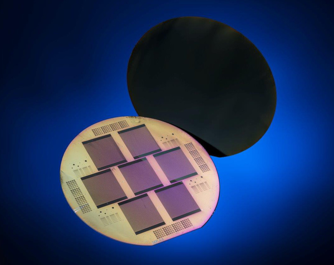
The record cell uses a passivating electron-selective n+-type polysilicon on oxide (POLO) junction at the minus contact of the cell and a hole-selective p+-type POLO junction at the plus contact. It is the high selectivity of theses junctions that allow such high efficiencies. These junctions are applied in an interdigitated pattern on the rear side. This minimizes the parasitic absorption in the poly-Si and avoids shading by front side metallization. n+-type and p+-type poly-Si are separated from each other by an intrinsic poly-Si region. The doped regions are structured using lab-type processes. However, the opening of the dielectric rear-side reflector is already done by an industrially feasible local laser ablation. The final objective is to integrate POLO junctions into the current mainstream technology with a clear advantage in efficiency. “Replacing photolithography by laser contact opening is a first important step towards industrialization as it enables screen-printing-based metallization”, states Prof. Robby Peibst, the leader of the workgroup.
The structured doping of the poly-Si was done at the Institute of Electronic Materials and Devices (Institut für Materialien und Bauelemente der Elektronik, MBE) at Leibniz Universität Hannover. ISFH and MBE gratefully acknowledge the contributions of the project partner Centrotherm who deposited the poly-Si layer in a LPCVD reactor. The partner Wacker contributed with knowledge of high-temperature processing of Si wafers.
The research at ISFH received financial support from the German Federal Ministry for Economic Affairs and Energy (BMWi) as well as from the State of Lower Saxony.
Additional notice:
A peer-reviewed paper with further details on the 26.1 % solar cell can be found here.

