Unsere Forschung
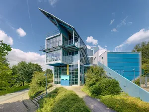
Herzlich willkommen am niedersächsischen Institut für Solarenergieforschung (ISFH)!
Die Energiewende braucht die Solarenergie. Solarenergie schont unser Klima, ist überall verfügbar, ist bei der Bevölkerung beliebt und erzeugt Strom und Wärme nahe dem Ort des Energiebedarfs. Und: Der weltweit rasante Ausbau der Solarenergie birgt große wirtschaftliche Chancen für unser Exportland!
Seit mehr als 30 Jahren fördern wir die Nutzung der Solarenergie durch unsere angewandte Forschung und die Ausbildung junger Menschen in den Bereichen „Photovoltaik“ und „Solare Systemtechnik“. Dabei ist „Innovation mit Wirkung“ unser Motto. Wir kooperieren intensiv mit der Industrie, mit anderen Forschungseinrichtungen und Universitäten und sind ein An-Institut der Leibniz Universität Hannover.
Wir freuen uns auf Ihre Anfragen, sei es als möglicher Forschungspartner aus der Industrie oder als Kunde unseres Dienstleistungsangebots oder in Form Ihrer Bewerbung für eine der ausgeschriebenen akademischen Abschlussarbeiten und Stellenangebote. Ihre Ideen zählen!
Aktuelle Meldungen
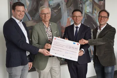
EFRE-Förderung stärkt Solar- und Wärmepumpenforschung in Niedersachsen
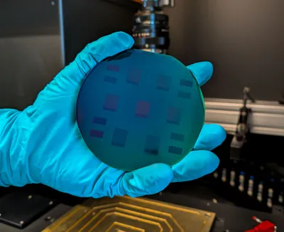
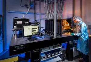
Meilenstein in der Tandem-Photovoltaik: 30,1 % Effizienz durch 3-Terminal-Architektur und ISFH POLO®-Technologie
POLO IBC Solarzellen: Wie das ISFH industrielle Wirkungsgrade von 24,5 Prozent erreicht und den Weg zu 26 Prozent vorbereitet
Neue Publikationen
Cell-to-module factors of perovskite/silicon tandem and silicon single junction mini modules for different module rear sides
Brockmann, T. L. and Blankemeyer, S. and Kirner, S. and Peibst, R. and Wietler, T. and Schulte-Huxel, H.Selective laser ablation of single layers from SiO2/poly-Si superlattices for patterning of 26 % efficient IBC solar cells
Römer, Udo and Rienäcker, Michael and Peibst, RobbyEnhanced Bandgap Flexibility in Perovskite-Silicon Tandem Solar Cells via Three-Terminal Architecture
Gholipoor, Mohammad and Rienaecker, Michael and Liu, Xuzheng and Orooji, Seyedamir and Fang, Lingyi and Fassl, Paul and Guo, Renjun and Lemmer, Uli and Peibst, Robby and Paetzold, Ulrich WilhelmFalling costs for battery storages make facade photovoltaic systems more attractive for prosumers
Bredemeier, Dennis and Mahner, Alexander and Wietler, Tobias and Niepelt, Raphael and Brendel, RolfIntegration of Laser–Patterned Photonic Crystals in Si Solar Cells
Rienäcker, Michael and Römer, Udo and Krügener, Jan and Maksimovic, Jovan and Katkus, Tomas and Stonytė, Dominyka and Ng, Soon Hock and Mu, Haoran and An Le, Nguyen Hoai and Khajehsaeidimahabadi, Zahra and Seniutinas, Gediminas and Baltrukonis, Justas and Ulcinas, Orestas and Mikutis, Mindaugas and Sabonis, Vytautas and Nishijima, Yoshiaki and John, Sajeev and Juodkazis, Saulius and Peibst, Robby and An Le, Nguyen HoaiAnstehende Termine
–
event_language_en
Hannover Messe, Halle 11, C33
Hannover Messe – Preview: Intensivkurs zu Poly-Si-Kontakten für TOPCon Solarzellen
Preview: Intensivkurs zu Poly-Si-Kontakten für TOPCon Solarzellen “Passivating contacts for TOPCon solar cells: Understanding and hands on practice - An intensive course at ISFH”
–
event_language_de
Hannover Messe, Halle 11, C33
Hannover Messe
Wir zeigen Forschung zu effizienten Solarzellen, Qualitätsprüfung in der Produktion und Photovoltaik in Gebäuden und Quartieren. Mit dabei: CityPV-Simulationen, DigiPV-Analysen, SQUIS-Inspektion und ein neuer TOPCon-Intensivkurs.
–
event_language_de
Institut für Solarenergieforschung
Nutzung von Industrie 4.0 und KI in der PV-Fertigung
Dr. Swaytha Sasidharan (ISC Konstanz) spricht über Industry 4.0 und Künstliche Intelligenz in der Photovoltaikfertigung und zeigt Ansätze zur digitalen Transformation von PV-Pilotlinien.
Forschung am ISFH
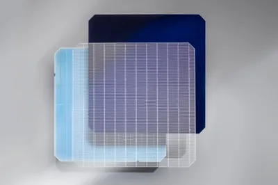
Siliziumsolarzellen und -module
Vom Silizium-Wafer bis zum PV-Modul: Unsere Forschung vereint Materialverständnis, Zell- und Modultechnologie, Qualitätssicherung und Fertigungstechnik für eine hocheffiziente, kostengünstige und ressourcenschonende Photovoltaik-Produktion.
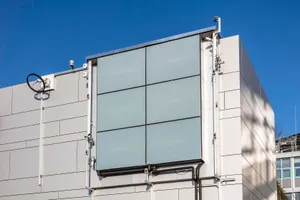
Gebäudeintegration
Gebäudeintegrierte Solarthermie, Photovoltaik und Photovoltaik-Thermie – funktional, ästhetisch und effizient. Wir entwickeln Lösungen für Fassaden, Dächer und neue Energieanwendungen.
Tandemsolarzellen und -module
Wir entwickeln innovative Tandemsolarzellen-Konzepte mit Fokus auf höchste Effizienz, industrielle Umsetzbarkeit und die Reindustrialisierung der PV-Produktion in Europa.
Gebäudeenergiesysteme
Innovative Energiesysteme für Gebäude: intelligent vernetzt, solar unterstützt und bereit für die klimaneutrale Zukunft.
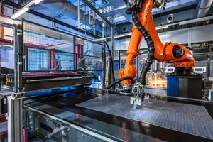
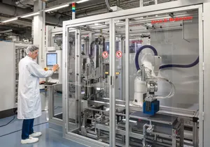
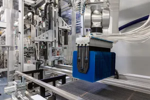
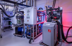
Fertigung und Spezialproduktion
Wir entwickeln am ISFH digitale, flexible und kosteneffiziente Technologien für die Produktion von Solarzellen und (maßgefertigten) PV-Modulen.
Wärmepumpen
Wir erforschen Wärmepumpen zur Versorgung von Gebäuden und Quartieren und thermischen Energiesystemen – mit Simulation, Komponentenanalyse und realen Praxistests.
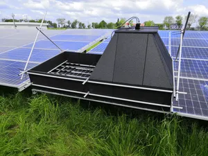
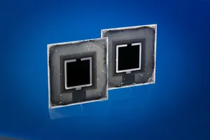
Zuverlässigkeit von Photovoltaik
Wir prüfen, wie zuverlässig neue Solarzellen, Materialien und PV-Module unter realen Bedingungen funktionieren, sei es im Labor, Freifeld oder mit Spezialmodulen.

Wasserstoff
Wir bringen grüne Wasserstofftechnologie voran: durch neue Katalysatoren, innovative Materialien mittels Protonen-Austausch-Membran-(PEM)-Elektrolyse und Unterstützung der Industrie bei der Skalierung neuer Lösungen.
Unser Service im CalTeC
Als von der DAkkS anerkanntes Labor bietet das ISFH CalTeC präzise Kalibrierungen und Prüfungen für Solarzellen, solarthermische Systeme, Spektroradiometer und Wärmepumpen nach internationalen Normen wie ISO, IEC und EN. Neben akkreditierten Services unterstützen wir Sie auch mit individuellen Prüfungen und Entwicklungsbegleitung.
Haben Sie eine Frage zum ISFH?
Wir helfen Ihnen gerne weiter! Sie können die konkreten Ansprechpartner zu unserer Forschung kontaktieren oder uns über unseren allgemeinen Kontakt erreichen.